Volume 141, Issue 1, March 2019
Structural Design of Land Grid Array Loading Mechanisms for Intel Central Processor Unit Stack Retention
Abstract
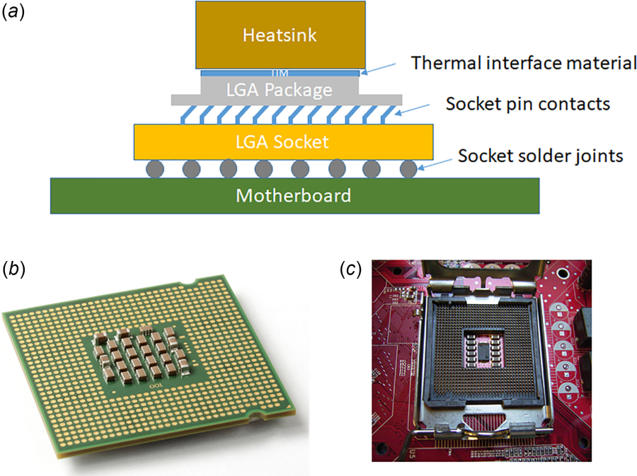
For more than a decade, land grid array (LGA) has been one of the main central processor unit (CPU) packages developed at Intel and AMD, and widely used in different computer systems. LGA loading mechanism has become more critical to achieve mechanical, thermal, and electrical functions with the increasing retention force requirement. During the development of the loading mechanisms for LGA packages and sockets, socket pin contact to LGA pad under retention load, solder joint reliability under shock load, socket pin fretting under vibration, and load degradation are some of the key structural risks. This paper reviews the structural designs of different loading mechanism solutions systematically and summarizes the key structural concerns and advantages. While the finite element analysis (FEA) was used to guide the design options in early platform architectural definition, this review discusses the evolution of Xeon LGA loading mechanisms developed at the Intel Data Center Group.
Authors
Citation
Geng, P. (February 25, 2019). "Structural Design of Land Grid Array Loading Mechanisms for Intel Central Processor Unit Stack Retention." ASME. J. Electron. Packag. March 2019; 141(1): 010801.
https://doi.org/10.1115/1.4042800
Liquid Cooling of Compute System
Abstract
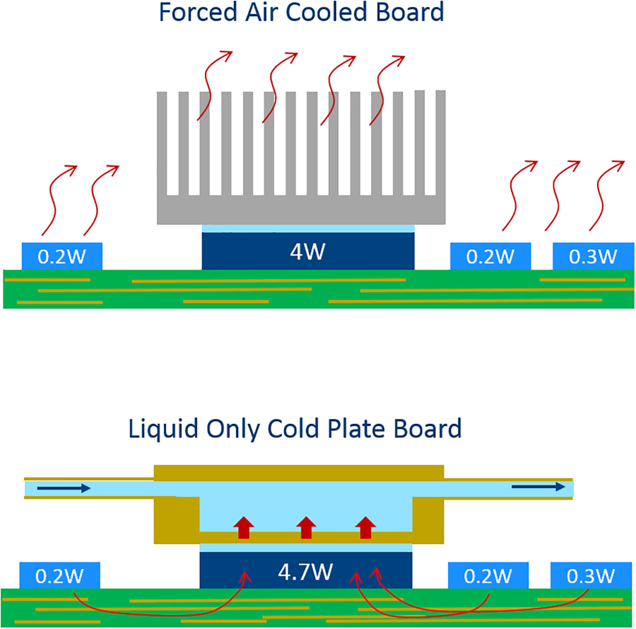
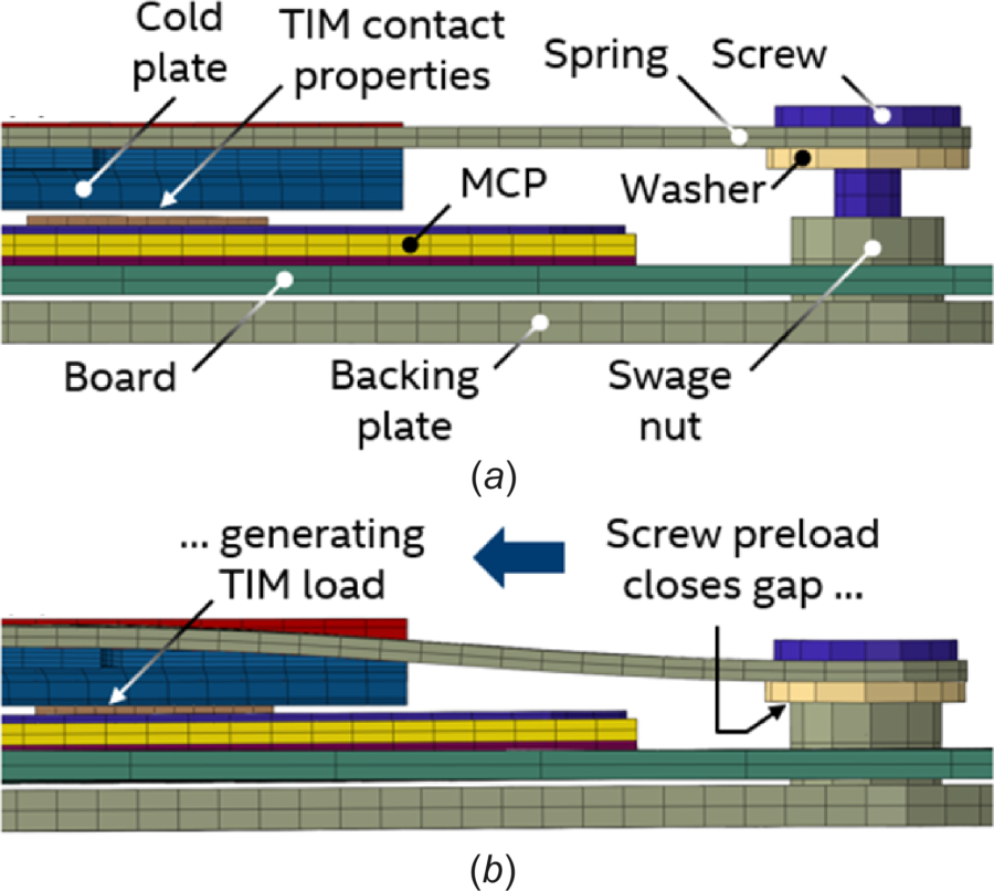
The continued demand for increasing compute performance results in an increasing system power and power density of many computers. The increased power requires more efficient cooling solutions than traditionally used air cooling. Therefore, liquid cooling, which has traditionally been used for large data center deployments, is becoming more mainstream. Liquid cooling can be used selectively to cool the high power components or the whole compute system. In this paper, the example of a fully liquid cooled server is used to describe different ingredients needed, together with the design challenges associated with them. The liquid cooling ingredients are cooling distribution unit (CDU), fluid, manifold, quick disconnects (QDs), and cold plates. Intel is driving an initiative to accelerate liquid cooling implementation and deployment by enabling the ingredients above. The functionality of these ingredients is discussed in this paper, while cold plates are discussed in detail.
Authors
Jessica Gullbrand; Mark J. Luckeroth; Mark E. Sprenger; Casey Winkel
Citation
Gullbrand, J., Luckeroth, M. J., Sprenger, M. E., and Winkel, C. (March 1, 2019). "Liquid Cooling of Compute System." ASME. J. Electron. Packag. March 2019; 141(1): 010802.
https://doi.org/10.1115/1.4042802
Thermomechanical Interaction Between Thin Bare-Die Package and Thermal Solution in Next-Generation Mobile Computing Platforms
Abstract
The demands for both thinner bare-die ball grid array (BGA) packages and thinner thermal solutions have added complexity for the thermal enabling design and material options associated with system on chip packages in mobile personal computer (PC) platforms. The thermomechanical interactions between the bare-die package and the thermal solution are very critical, creating the needs for: (1) an in-depth thermomechanical characterization to understand their impacts on product quality and performance and (2) a simple and yet robust modeling methodology to analyze design parameters using a commercially available software. In this paper, experimental metrologies and modeling methodology are developed with the details of contents documented. Validation of the newly developed tools and recommendation/guidance are also discussed for detailed assessments of thermomechanical tradeoffs for optimal design spaces for next-generation mobile platforms.
Authors
Aastha Uppal; Jerrod Peterson; Je-Young Chang; Xi Guo; Frank Liang; Weihua Tang
Citation
Uppal, A., Peterson, J., Chang, J., Guo, X., Liang, F., and Tang, W. (March 4, 2019). "Thermomechanical Interaction Between Thin Bare-Die Package and Thermal Solution in Next-Generation Mobile Computing Platforms." ASME. J. Electron. Packag. March 2019; 141(1): 010803.
https://doi.org/10.1115/1.4042801
Volume 141, Issue 2, June 2019
Thermal Management and Characterization of High-Power Wide-Bandgap Semiconductor Electronic and Photonic Devices in Automotive Applications
Abstract
GaN-based high-power wide-bandgap semiconductor electronics and photonics have been considered as promising candidates to replace conventional devices for automotive applications due to high energy conversion efficiency, ruggedness, and superior transient performance. However, performance and reliability are detrimentally impacted by significant heat generation in the device active area. Therefore, thermal management plays a critical role in the development of GaN-based high-power electronic and photonic devices. This paper presents a comprehensive review of the thermal management strategies for GaN-based lateral power/RF transistors and light-emitting diodes (LEDs) reported by researchers in both industry and academia. The review is divided into three parts: (1) a survey of thermal metrology techniques, including infrared thermography, Raman thermometry, and thermoreflectance thermal imaging, that have been applied to study GaN electronics and photonics; (2) practical thermal management solutions for GaN power electronics; and (3) packaging techniques and cooling systems for GaN LEDs used in automotive lighting applications.
Authors
Seung Kyu Oh; James Spencer Lundh; Shahab Shervin; Bikramjit Chatterjee; Dong Kyu Lee; Sukwon Choi; Joon Seop Kwak; Jae-Hyun Ryou
Citation
Oh, S. K., Lundh, J. S., Shervin, S., Chatterjee, B., Lee, D. K., Choi, S., Kwak, J. S., and Ryou, J. (February 25, 2019). "Thermal Management and Characterization of High-Power Wide-Bandgap Semiconductor Electronic and Photonic Devices in Automotive Applications." ASME. J. Electron. Packag. June 2019; 141(2): 020801.
https://doi.org/10.1115/1.4041813
Volume 141, Issue 4, December 2019
Recent Advances and Trends in Fan-Out Wafer/Panel-Level Packaging
Abstract
The recent advances and trends in fan-out wafer/panel-level packaging (FOW/PLP) are presented in this study. Emphasis is placed on: (A) the package formations such as (a) chip first and die face-up, (b) chip first and die face-down, and (c) chip last or redistribution layer (RDL)-first; (B) the RDL fabrications such as (a) organic RDLs, (b) inorganic RDLs, (c) hybrid RDLs, and (d) laser direct imaging (LDI)/printed circuit board (PCB) Cu platting and etching RDLs; (C) warpage; (D) thermal performance; (E) the temporary wafer versus panel carriers; and (F) the reliability of packages on PCBs subjected to thermal cycling condition. Some opportunities for FOW/PLP will be presented.
Authors
Citation
Lau, J. H. (May 17, 2019). "Recent Advances and Trends in Fan-Out Wafer/Panel-Level Packaging." ASME. J. Electron. Packag. December 2019; 141(4): 040801.
https://doi.org/10.1115/1.4043341
A State-of-the-Art Review of Fatigue Life Prediction Models for Solder Joint
Abstract
Fatigue failure of solder joints is one of the major causes of failure in electronic devices. Fatigue life prediction models of solder joints were first put forward in the early 1960s, and since then, numbers of methods were used to model the fatigue mechanism of solder joints. In this article, the majority fatigue life models are summarized, with emphasis on the latest developments in the fatigue life prediction methods. All the models reviewed are grouped into four categories based on the factors affecting the fatigue life of solder joints, which are: plastic strain-based fatigue models, creep damage-based fatigue models, energy-based fatigue models, and damage accumulation-based fatigue models. The models that do not fit any of the above categories are grouped into “other models.” Applications and potential limitations for those models are also discussed.
Authors
Sinan Su; Francy John Akkara; Ravinder Thaper; Atif Alkhazali; Mohammad Hamasha; Sa'd Hamasha
Citation
Su, S., Akkara, F. J., Thaper, R., Alkhazali, A., Hamasha, M., and Hamasha, S. (May 17, 2019). "A State-of-the-Art Review of Fatigue Life Prediction Models for Solder Joint." ASME. J. Electron. Packag. December 2019; 141(4): 040802.
https://doi.org/10.1115/1.4043405
Embedded Cooling for Wide Bandgap Power Amplifiers: A Review
Abstract
Successful utilization of the inherent capability of wide bandgap materials and architectures for radio frequency (RF) power amplifiers (PAs) necessitates the creation of an alternative thermal management paradigm. Recent “embedded cooling” efforts in the aerospace industry have focused on overcoming the near-junction thermal limitations of conventional electronic materials and enhancing removal of the dissipated power with on-chip cooling. These efforts, focusing on the use of diamond substrates and microfluidic jet impingement, are ushering in a new generation (Gen3) of thermal packaging technology. Following the introduction of a modified Johnson's figure-of-merit (JFOM-k), which includes thermal conductivity to reflect the near-junction thermal limitation, attention is turned to the options, challenges, and techniques associated with the development of embedded thermal management technology (TMT). Record GaN-on-Diamond transistor linear power of 11 W/mm, transistor power fluxes in excess of 50 kW/cm2, and heat fluxes, above 40 kW/cm2, achieved in Defense Advanced Research Projects Agency (DARPA)'s near-junction thermal transport (NJTT) program, are described. Raytheon's ICECool demonstration monolithic microwave integrated circuits (MMICs), which achieved 3.1× the CW RF power output and 4.8× the CW RF power density relative to a baseline design, are used to illustrate the efficacy of Gen3 embedded cooling.
Authors
A. Bar Cohen; J. J. Maurer; D. H. Altman
Citation
Bar-Cohen, A., Maurer, J. J., and Altman, D. H. (July 30, 2019). "Embedded Cooling for Wide Bandgap Power Amplifiers: A Review." ASME. J. Electron. Packag. December 2019; 141(4): 040803.
https://doi.org/10.1115/1.4043404
Progress and Perspective of Near-Ultraviolet and Deep-Ultraviolet Light-Emitting Diode Packaging Technologies
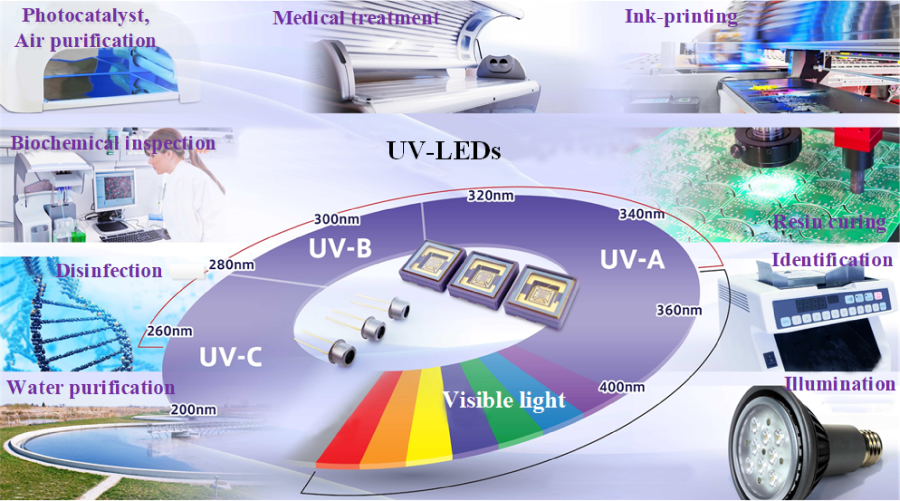
Abstract
Ultraviolet light-emitting diodes (UV-LEDs) have drawn considerable attention in environment, life science, and industry fields, such as the applications of near UV-LEDs in resin curing, illumination, and identification, and deep UV-LEDs in disinfection, medical treatment, and biochemical inspection. However, due to the limitation of packaging technology, UV-LED devices exhibit low light efficiency and poor reliability compared with visible LEDs. The organic encapsulation materials are prone to UV aging, thermal degradation, and nonairtightness, which significantly reduce the performances of UV-LEDs. In order to solve this issue, UV-LED packaging technology has been proposed for UV-LED devices instead of conventional LED packaging. In this review, we investigated in detail the overview and challenges of near-ultraviolet light-emitting diodes (NUV-LED)/deep-ultraviolet light-emitting diodes (DUV-LED) packaging. For the packaging of UV-LEDs, all inorganic encapsulation materials, hermetic packaging structures with low-temperature bonding, reduced reflection losses, UV stable and transparent materials, and effective thermal management are key progresses to enhance the light efficiency and reliability of UV-LEDs. In addition, the summary and perspectives of NUVLED/DUV-LED packaging were introduced and discussed.
Authors
Yang Peng; Renli Liang; Yun Mou; Jiangnan Dai; Mingxiang Chen; Xiaobing Luo
Citation
Peng, Y., Liang, R., Mou, Y., Dai, J., Chen, M., and Luo, X. (September 19, 2019). "Progress and Perspective of Near-Ultraviolet and Deep-Ultraviolet Light-Emitting Diode Packaging Technologies." ASME. J. Electron. Packag. December 2019; 141(4): 040804.
https://doi.org/10.1115/1.4044624
Volume 142, Issue 1, March 2020
Packaging for Laser-Based White Lighting: Status and Perspectives
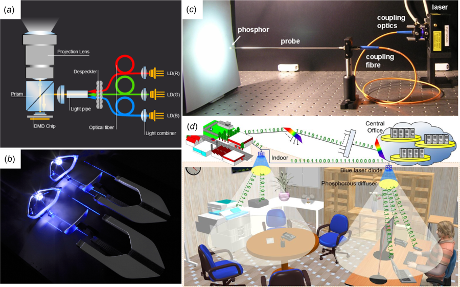
Abstract
Light-emitting diodes (LEDs) have gained wide adoption in general illumination applications in the last decade. However, the efficiency drop of LEDs with increasing current density limits the luminous flux per wafer area. In contrast, laser diodes (LDs) can achieve higher efficiency at high current density. Likewise, the etendue of LDs is very low due to the small emitting area and divergent angle, facilitating the high-luminance. Hence, LDs may outperform LEDs in future high-luminance solid-state lighting (SSL). However, the rapid development of high-luminance white laser diode (WLD) is still facing some challenges. First, the heat flux of LD chip is extremely high, leading to a higher junction temperature. Second, the laser beam exhibits an elliptical and astigmatic pattern with Gaussian intensity distribution, which may deteriorate the lighting performances. Third, to achieve high-luminance lighting, the laser beam is usually focused onto the phosphor layer, which may easily increase the phosphor temperature to the thermal quenching region. A comprehensive understanding of these problems enables the advancements of packaging designs for WLDs. In this review, we summarized the recent progress in the packaging of WLDs. First, the advantages and applications of LDs were presented. Then, the state-of-the-art methods of generating white light using LDs were reviewed, in terms of packaging structures and performances. Finally, the challenges and corresponding progresses for the packaging of WLDs were overviewed. This review intends to contribute to the development of next-generation high-luminance laser-based white lighting.
Authors
Citation
Ma, Y., and Luo, X. (September 19, 2019). "Packaging for Laser-Based White Lighting: Status and Perspectives." ASME. J. Electron. Packag. March 2020; 142(1): 010801.
https://doi.org/10.1115/1.4044359
Volume 142, Issue 4, December 2020
Comparative Study on Power Module Architectures for Modularity and Scalability
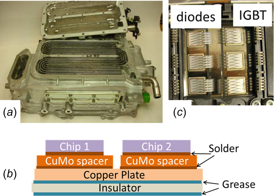
Abstract
Silicon carbide (SiC) wide bandgap power electronics are being applied in hybrid electric vehicle (HEV) and electrical vehicles (EV). The Department of Energy (DOE) has set target performance goals for 2025 to promote EV and HEV as a means of carbon emission reduction and long-term sustainability. Challenges include higher expectations on power density, performance, efficiency, thermal management, compactness, cost, and reliability. This study will benchmark state of the art silicon and SiC technologies. Power modules used in commercial traction inverters are analyzed for their within-package first-level interconnect methods, module architecture, and integration with cooling structure. A few power module package architectures from both industry-adopted standards and proposed patented technologies are compared in modularity and scalability for integration into inverters. The current trends of power module architectures and their integration into inverter are also discussed. The development of an eco-system to support the wide bandgap semiconductors-based power electronics is highlighted as an ongoing challenge.
Authors
Citation
Lu, M. (June 29, 2020). "Comparative Study on Power Module Architectures for Modularity and Scalability." ASME. J. Electron. Packag. December 2020; 142(4): 040801.
https://doi.org/10.1115/1.4047472
Volume 143, Issue 1, March 2021
Recent Advances in Thermal Metamaterials and Their Future Applications for Electronics Packaging
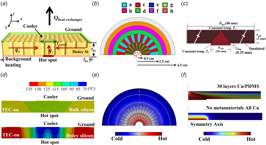
Abstract
Thermal metamaterials exhibit thermal properties that do not exist in nature but can be rationally designed to offer unique capabilities of controlling heat transfer. Recent advances have demonstrated successful manipulation of conductive heat transfer and led to novel heat guiding structures such as thermal cloaks, concentrators, etc. These advances imply new opportunities to guide heat transfer in complex systems and new packaging approaches as related to thermal management of electronics. Such aspects are important, as trends of electronics packaging toward higher power, higher density, and 2.5D/3D integration are making thermal management even more challenging. While conventional cooling solutions based on large thermal-conductivity materials as well as heat pipes and heat exchangers may dissipate the heat from a source to a sink in a uniform manner, thermal metamaterials could help dissipate the heat in a deterministic manner and avoid thermal crosstalk and local hot spots. This paper reviews recent advances of thermal metamaterials that are potentially relevant to electronics packaging. While providing an overview of the state-of-the-art and critical 2.5D/3D-integrated packaging challenges, this paper also discusses the implications of thermal metamaterials for the future of electronic packaging thermal management. Thermal metamaterials could provide a solution to nontrivial thermal management challenges. Future research will need to take on the new challenges in implementing the thermal metamaterial designs in high-performance heterogeneous packages to continue to advance the state-of-the-art in electronics packaging.
Authors
Jae Choon Kim; Zongqing Ren; Anil Yuksel; Ercan M. Dede; Prabhakar R. Bandaru; Dan Oh; Jaeho Lee
Citation
Kim, J. C., Ren, Z., Yuksel, A., Dede, E. M., Bandaru, P. R., Oh, D., and Lee, J. (June 29, 2020). "Recent Advances in Thermal Metamaterials and Their Future Applications for Electronics Packaging." ASME. J. Electron. Packag. March 2021; 143(1): 010801.
https://doi.org/10.1115/1.4047414
Volume 143, Issue 2, June 2021
Review of Methodologies for Structural Integrity Evaluation of Power Modules
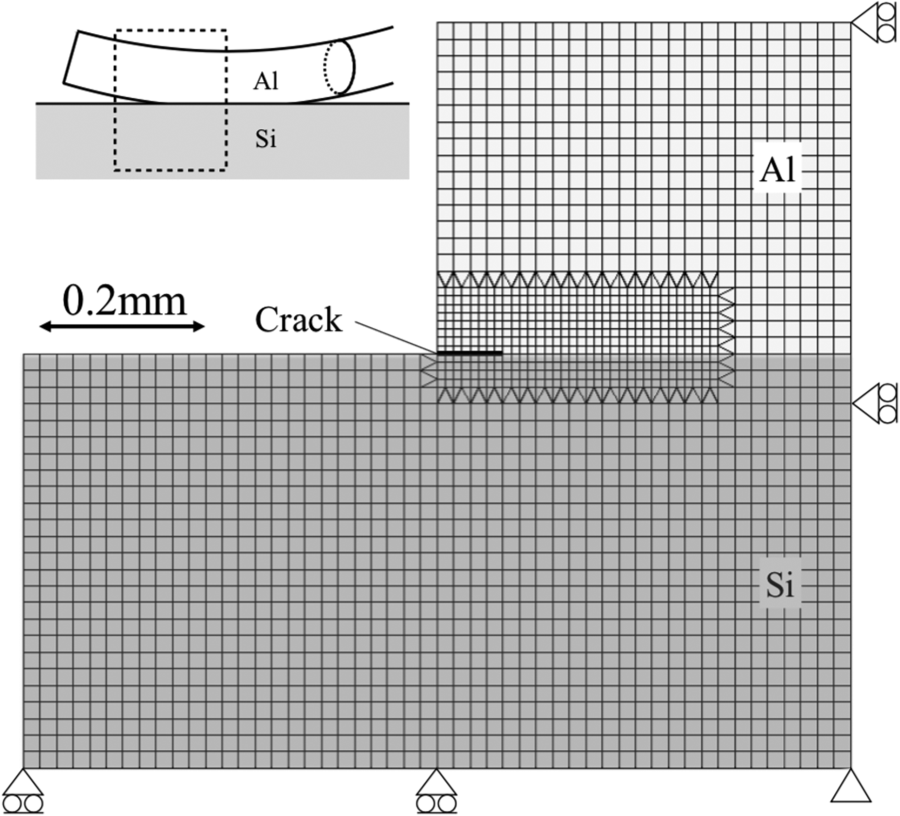
Abstract
This paper reviews the previous research on the methodologies for evaluating structural integrity of wire bonds and die-attachments in power modules. Under power module operation, these parts are subjected to repeated temperature variations which induce repeated thermal stress due to the mismatch in coefficients of thermal expansion (CTE) of the constituent materials. Thus, thermal fatigue phenomena are critical issues for the structural integrity of power modules. In the present paper, we also deal with the evaluation methodologies for thermal fatigue in the temperatures over 200oC which are expected operational temperatures for wide bandgap semiconductor power modules. The failure models based on the temperature range ΔT widely used in the power electronics community are critically reviewed from a mechanical engineering viewpoint. Detailed discussion is given concerning the superiority of failure models based on the physical quantities such as the inelastic strain range Δεin; , the inelastic strain energy density range ΔWin , and the nonlinear fracture mechanics parameter range ΔT * over the conventional ΔT -based failure models. It is also pointed out that the distributed state concept (DSC) approaches based on the unified constitutive modeling and the unified mechanics theory are promising for evaluating the structural integrity of power modules. Two kinds of test methods, a power cycling test (PCT) and a thermal cycling test (TCT), are discussed in the relation to evaluating the lifetimes of wire-liftoff and die attach cracking.
Authors
Noriyuki Miyazaki; Nobuyuki Shishido; Yutaka Hayama
Citation
Miyazaki, N., Shishido, N., and Hayama, Y. (August 27, 2020). "Review of Methodologies for Structural Integrity Evaluation of Power Modules." ASME. J. Electron. Packag. June 2021; 143(2): 020801.
https://doi.org/10.1115/1.4048038
A Review on United States Patents to Prevent Mechanical Failures in Foldable Smartphones
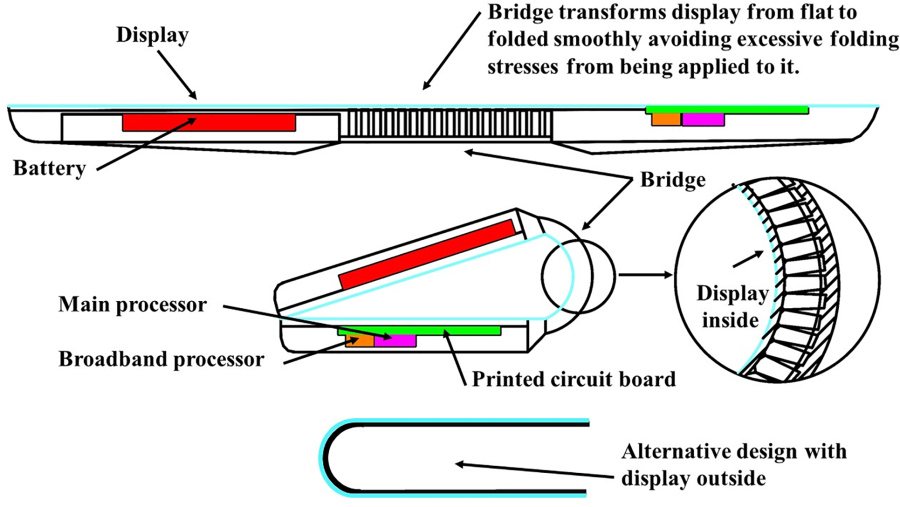
Abstract
A foldable smartphone is an exciting new approach for future mobile systems. With some early models being introduced to the market, research and development is being performed to increase the reliability of future systems. Mechanical failure of the display is the major source of foldable smartphone's reliability issues. The display is a laminate structure including an organic light emitting diode (OLED) layer (emission layer and pixel electrode layer), a touch panel, a polarizer, and multiple protective layers in addition to multiple functional coatings and supporting structures. The display is exposed to repeated folding, finger touch, and the impact of external sharp objects. In addition, mechanical behavior changes through the thickness of the display; which adds extra challenges in preventing damage to vital components of the display. This review covers more than 100 U.S. patents about the mechanical failures in foldable smartphones published or filed after 2015. Different inventions reviewed are to design a foldable configuration to prevent mechanical failures resulting from the following four mechanisms: (1) plastic deformation (yielding, creep, and fatigue); (2) fracture; (3) delamination; and (4) buckling (warping, buckling, wrinkling, and creasing).
Authors
Ali Nematollahisarvestani; Yung-Cheng “Y. C.” Lee
Citation
Nematollahisarvestani, A., and Lee, Y. “. C. (September 3, 2020). "A Review on United States Patents to Prevent Mechanical Failures in Foldable Smartphones." ASME. J. Electron. Packag. June 2021; 143(2): 020802.
https://doi.org/10.1115/1.4048011
State of the Art of Lead-Free Solder Joint Reliability
Abstract
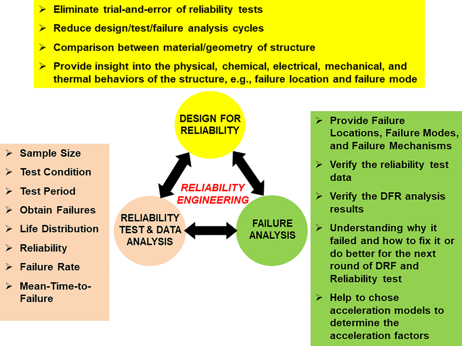
The state of the art of lead-free solder joint reliability is investigated in this study. Emphasis is placed on the design for reliability (DFR) and reliability testing and data analysis. For DFR: (a) the Norton power creep constitutive equations and examples for Au20Sn, Sn58Bi, Sn3.8Ag0.7Cu, and Sn3.8Ag0.7Cu0.03Ce, (b) the Wises two power creep constitutive equations and examples for Sn3.5Ag and Sn4Ag0.5Cu, (c) the Garofalo hyperbolic sine creep constitutive equations and examples for Sn3.5Ag, Sn3Ag0.5Cu, Sn3.9Ag0.6Cu, Sn3.8Ag0.7Cu, Sn3.5Ag0.5Cu, and Sn3.5Ag0.75Cu, Sn4Ag0.5Cu, Sn(3.5-3.9)Ag(0.5-0.8)Cu, 100In, Sn52In, Sn3.8Ag0.7Cu0.03Ce, and Au20Sn, and (d) the Anand viscoplasticity constitutive equations and examples for Sn3.5Ag, Sn3Ag0.5Cu, Sn3.8Ag0.7Cu, Sn3.8Ag0.7CuCe, Sn3.8Ag0.7CuAl, Au20Sn, Sn3.5Ag with temperature and strain rate-dependent parameters, and Sn1Ag0.5Cu, Sn2Ag0.5Cu, Sn3Ag0.5Cu, and Sn4Ag0.5Cu after extreme aging will be discussed. For reliability testing and data analysis: (a) the Weibull and lognormal life distributions for lead-free solder joints under thermal-cycling and drop tests, (b) the true Weibull slope, true characteristic life, and true mean life, and (c) the linear acceleration factors for various lead-free solder alloys based on: (i) frequency and maximum temperature, (ii) dwell time and maximum temperature, and (iii) frequency and mean temperature will be presented. Some recommendations will also be provided.
Authors
Citation
Lau, J. H. (September 3, 2020). "State of the Art of Lead-Free Solder Joint Reliability." ASME. J. Electron. Packag. June 2021; 143(2): 020803.
https://doi.org/10.1115/1.4048037
Volume 143, Issue 3, September 2021
A Review of Thermo-Hydraulic Performance of Metal Foam and Its Application as Heat Sinks for Electronics Cooling
Abstract
High porosity metal foams offer large surface area per unit volume and have been considered as effective candidates for convection heat transfer enhancement, with applications as heat sinks in electronics cooling. In this paper, the research progress in thermohydraulic performance characterization of metal foams and their application as heat sinks for electronics cooling are reviewed. We focus on buoyancy-induced convection, forced convection, flow boiling, and solid/liquid phase change using phase change materials (PCMs). Under these heat transfer conditions, the effects of various parameters influencing the performance of metal foam heat sink are discussed. It is concluded that metal foams demonstrate promising capability for heat transfer augmentation, but some key issues still need to be investigated regarding the fundamental mechanisms of heat transfer to enable the development of more efficient and compact heat sinks.
Authors
Yongtong Li; Liang Gong; Minghai Xu; Yogendra Joshi
Citation
Li, Y., Gong, L., Xu, M., and Joshi, Y. (January 19, 2021). "A Review of Thermo-Hydraulic Performance of Metal Foam and Its Application as Heat Sinks for Electronics Cooling." ASME. J. Electron. Packag. September 2021; 143(3): 030801.
https://doi.org/10.1115/1.4048861
Volume 144, Issue 1, March 2022
A Review on Transient Thermal Management of Electronic Devices
Abstract
Much effort in the area of electronics thermal management has focused on developing cooling solutions that cater to steady-state operation. However, electronic devices are increasingly being used in applications involving time-varying workloads. These include microprocessors (particularly those used in portable devices), power electronic devices such as insulated gate bipolar transistors (IGBTs), and high-power semiconductor laser diode arrays. Transient thermal management solutions become essential to ensure the performance and reliability of such devices. In this review, emerging transient thermal management requirements are identified, and cooling solutions reported in the literature for such applications are presented with a focus on time scales of thermal response. Transient cooling techniques employing actively controlled two-phase microchannel heat sinks, phase change materials (PCM), heat pipes/vapor chambers, combined PCM-heat pipes/vapor chambers, and flash boiling systems are examined in detail. They are compared in terms of their thermal response times to ascertain their suitability for the thermal management of pulsed workloads associated with microprocessor chips, IGBTs, and high-power laser diode arrays. Thermal design guidelines for the selection of appropriate package level thermal resistance and capacitance combinations are also recommended.
Authors
Citation
Mathew, J., and Krishnan, S. (August 6, 2021). "A Review on Transient Thermal Management of Electronic Devices." ASME. J. Electron. Packag. March 2022; 144(1): 010801.
https://doi.org/10.1115/1.4050002
Spray Cooling on Enhanced Surfaces: A Review of the Progress and Mechanisms
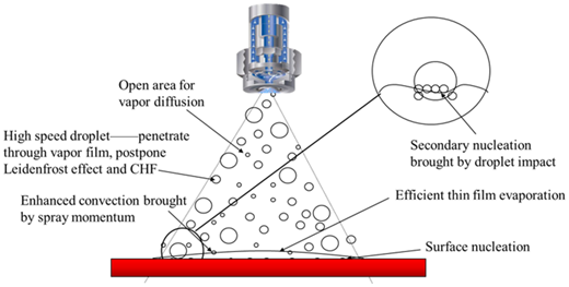
Abstract
The rapid development of high-power electronic, energy, and propulsion systems has led us to the point where the performances of these systems are limited by their cooling capacities. Current electronics can generate heat fluxes up to 10–100 W/cm2, and heat flux over 1000 W/cm2 needs to be dissipated with a minimum coolant flow rate in next-generation power electronics. The multiple efficient heat transfer mechanisms have made spray cooling a high heat flux, uniform and efficient cooling technique proven effective in various applications. However, the cooling capacity and efficiency of spray cooling need to be further improved to meet the demands of next-generation ultrahigh-power applications. Engineering of surface properties and structures, which is enabled by state-of-the-art manufacturing techniques, can fundamentally affect the liquid–wall interactions in spray cooling, thus becoming the most promising way to enhance spray cooling. However, the mechanisms of surface-enhanced spray cooling are diverse and ambiguous, causing a lack of clear guiding principles for engineered surface design. Here, the progress in surface engineering-enhanced spray cooling is reviewed for surface structures of millimeter, micrometer, and nanometer scales and hierarchical structured surfaces, and the performances from the reviewed literature are evaluated and compared. The reviewed data show that spray cooling can achieve a critical heat flux (CHF) above 945.7 W/cm2 and a heat transfer coefficient (HTC) up to 57 W/cm2K on structured surfaces without the assistance of secondary gas flow and a CHF and an HTC up to 1250.1 W/cm2 and 250 W/cm2K, respectively, on a smooth surface with the assistance of secondary gas flow. A CHF enhancement up to 110% was achieved on a hybrid micro- and nanostructured surface. A clear map of enhancement mechanisms related to the scales of surface structures is proposed, which can help the design of engineered surfaces in spray cooling. Some future concerns are proposed as well. This work helps the understanding and design of engineered surfaces in spray cooling and provides insights for interdisciplinary applications of heat transfer and advanced engineering materials.
Authors
Ruina Xu; Gaoyuan Wang; Peixue Jiang
Citation
Xu, R., Wang, G., and Jiang, P. (August 6, 2021). "Spray Cooling on Enhanced Surfaces: A Review of the Progress and Mechanisms." ASME. J. Electron. Packag. March 2022; 144(1): 010802.
https://doi.org/10.1115/1.4050046
Underfill Flow in Flip-Chip Encapsulation Process: A Review
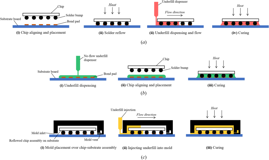
Abstract
The scope of review of this paper focused on the precuring underfilling flow stage of encapsulation process. A total of 80 related works has been reviewed and being classified into process type, method employed, and objective attained. Statistically showed that the conventional capillary is the most studied underfill process, while the numerical simulation was mainly adopted. Generally, the analyses on the flow dynamic and distribution of underfill fluids in the bump array aimed for the filling time determination as well as the predictions of void occurrence. Parametric design optimization was subsequently conducted to resolve the productivity issue of long filling time and reliability issue of void occurrence. The bump pitch was found to the most investigated parameter, consistent to the miniaturization demand. To enrich the design versatility and flow visualization aspects, experimental test vehicle was innovated using imitated chip and replacement fluid, or even being scaled-up. Nonetheless, the analytical filling time models became more accurate and sophiscasted over the years, despite still being scarce in number. With the technological advancement on analysis tools and further development of analytic skills, it was believed that the future researches on underfill flow will become more comprehensive, thereby leading to the production of better packages in terms of manufacturing feasibility, performances, and reliability. Finally, few potential future works were recommended, for instance, microscopic analysis on the bump–fluid interaction, consideration of filler particles, and incorporation of artificial intelligence.
Authors
Fei Chong Ng; Mohamad Aizat Abas
Citation
Ng, F. C., and Abas, M. A. (August 6, 2021). "Underfill Flow in Flip-Chip Encapsulation Process: A Review." ASME. J. Electron. Packag. March 2022; 144(1): 010803.
https://doi.org/10.1115/1.4050697
Volume 144, Issue 2, June 2022
Advancement of Chip Stacking Architectures and Interconnect Technologies for Image Sensors
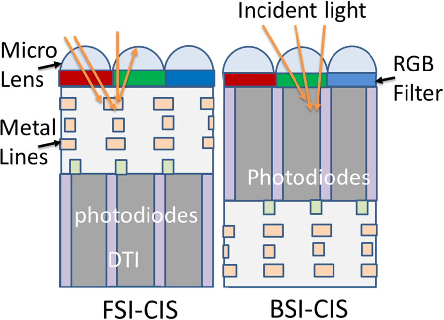
Abstract
Numerous technology breakthroughs have been made in image sensor development in the past two decades. Image sensors have evolved into a technology platform to support many applications. Their successful implementation in mobile devices has accelerated market demand and established a business platform to propel continuous innovation and performance improvement extending to surveillance, medical, and automotive industries. This overview briefs the general camera module and the crucial technology elements of chip stacking architectures and advanced interconnect technologies. This study will also examine the role of pixel electronics in determining the chip stacking architecture and interconnect technology of choice. It is conducted by examining a few examples of CMOS image sensors (CIS) for different functions such as visible light detection, single photon avalanche photodiode (SPAD) for low light detection, rolling shutter, and global shutter, and depth sensing and light detection and ranging (LiDAR). Performance attributes of different architectures of chip stacking are overviewed. Direct bonding followed by Via-last through silicon via (Via-last TSV) and hybrid bonding (HB) technologies are identified as newer and favorable chip-to-chip interconnect technologies for image sensor chip stacking. The state-of-the-art ultrahigh-density interconnect manufacturability is also highlighted.
Authors
Citation
Lu, M. (September 24, 2021). "Advancement of Chip Stacking Architectures and Interconnect Technologies for Image Sensors." ASME. J. Electron. Packag. June 2022; 144(2): 020801.
https://doi.org/10.1115/1.4052069
Volume 144, Issue 3, September 2022
Effects of Gaseous and Particulate Contaminants on Information Technology Equipment Reliability—A Review
Abstract
Over the last decade, several hyper-scale data center companies such as Google, Facebook, and Microsoft have demonstrated the cost-saving capabilities of airside economization with direct/indirect heat exchangers by moving to chiller-less air-cooled data centers. Under pressure from data center owners, information technology equipment OEMs like Dell and IBM are developing information technology equipment that can withstand peak excursion temperature ratings of up to 45 °C, clearly outside the recommended envelope, and into ASHRAEs A4 allowable envelope. As popular and widespread as these cooling technologies are becoming, airside economization comes with its challenges. There is a risk of premature hardware failures or reliability degradation posed by uncontrolled fine particulate and gaseous contaminants in presence of temperature and humidity transients. This paper presents an in-depth review of the particulate and gaseous contamination-related challenges faced by the modern-day data center facilities that use airside economization. This review summarizes specific experimental and computational studies to characterize the airborne contaminants and associated failure modes and mechanisms. In addition, standard lab-based and in-situ test methods for measuring the corrosive effects of the particles and the corrosive gases, as the means of testing the robustness of the equipment against these contaminants, under different temperature and relative humidity conditions are also reviewed. It also outlines the cost-sensitive mitigation techniques like improved filtration strategies and methods that can be utilized for efficient implementation of airside economization.
Authors
Satyam Saini; Jimil M. Shah; Pardeep Shahi; Pratik Bansode; Dereje Agonafer; Prabjit Singh; Roger Schmidt; Mike Kaler
Citation
Saini, S., Shah, J. M., Shahi, P., Bansode, P., Agonafer, D., Singh, P., Schmidt, R., and Kaler, M. (September 15, 2021). "Effects of Gaseous and Particulate Contaminants on Information Technology Equipment Reliability—A Review." ASME. J. Electron. Packag. September 2022; 144(3): 030801.
https://doi.org/10.1115/1.4051255
Recent Developments in Air Pumps for Thermal Management of Electronics
Abstract
For electronics, poor thermal management could cause severe mechanical and electrical failures. Forced convective air cooling, i.e., flowing air over a hot surface, is one of the most efficient and economical solutions to manage thermal issues of electronics. Air pump is used to initiate and sustain airflow required in forced convection. This paper reviews both the mechanical and the nonmechanical air pumps that have been using widely in current electronics or have a great potential in future electronics. The mechanical pumps include axial fans, blowers, beam fans, and diaphragm pumps, while the nonmechanical pump specifically focuses on electrohydrodynamic pumps. This paper presents the working principle first and then the recent developments, including the pump itself (design, characteristics, etc.) and the applications in thermal management (placement, integration, etc.). In the end, this paper conducts the strength analysis (flow rate, pressure, noise, flexibility, and reliability) among the reviewed five types of air pumps.
Authors
Citation
Wen, T., and Ye, J. (October 1, 2021). "Recent Developments in Air Pumps for Thermal Management of Electronics." ASME. J. Electron. Packag. September 2022; 144(3): 030802.
https://doi.org/10.1115/1.4051970
Volume 144, Issue 4, December 2022
Parametric Effects on Pool Boiling Heat Transfer and Critical Heat Flux: A Critical Review
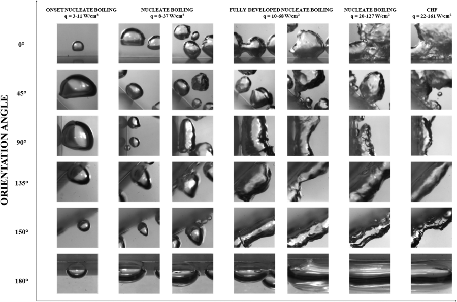
Abstract
Pool boiling heat transfer offers high-performance cooling opportunities for thermal problems of electronics limited with high heat fluxes. Therefore, many researchers have been extensively studying over the last six decades. This paper presents a critical literature review of various parametric effects on pool boiling heat transfer and critical heat flux (CHF) such as pressure, subcooling, surface topography, surface orientation, working fluid, and combined effects. To achieve an optimal heat removal solution for a particular problem, each of these parameters must be understood. The governing mechanisms are discussed separately, and various options related to the selection of appropriate working fluids are highlighted. A broad summary of correlations developed until now for predicting CHF is presented with their ranges of validity. While proposed correlations for predicting CHF have been quite promising, they still have a considerable uncertainty (±25%). Finally, a correlation proposed by Professor Avram Bar-Cohen and his team (thermal management of electronics (TME) correlation) is compared with the experimental dataset published in previous studies. It shows that the uncertainty band can be further narrowed down to ±12.5% for dielectric liquids by using TME correlation. Furthermore, this correlation has been enhanced to predict CHF values underwater above 50 W/cm2 by applying a genetic algorithm, and new perspectives for possible future research activities are proposed.
Authors
Tolga Emir; Hamza Ourabi; Mete Budakli; Mehmet Arik
Citation
Emir, T., Ourabi, H., Budakli, M., and Arik, M. (April 28, 2022). "Parametric Effects on Pool Boiling Heat Transfer and Critical Heat Flux: A Critical Review." ASME. J. Electron. Packag. December 2022; 144(4): 040801.
https://doi.org/10.1115/1.4054184
Volume 145, Issue 2, June 2023
Failure Mechanisms Driven Reliability Models for Power Electronics: A Review
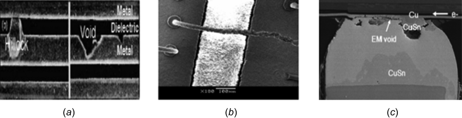
Abstract
Miniaturization as well as manufacturing processes that electronics devices are subjected to often results in to increase in operational parameters such as current density, temperature, mechanical load, and with potential to induce stresses that may be detrimental to device reliability. Past studies have identified some failure mechanisms common to these devices. Examples of these failure mechanisms include fatigue, electromigration, stress induced voiding, corrosion, conduction filament formation, and time-dependent dielectric breakdown. While some review activities related to reliability model development based on these failure mechanisms can be easily found in literature, to the best of our knowledge, a single review paper, which captures the reliability model progresses made over the past four decades across these failure mechanisms in comparison with Standards such as Joint Electron Device Engineering Council (JEDEC) and Institute for Printed Circuits (IPC) is to the best of our knowledge lacking. To fill this gap, a detailed review of failure mechanism driven reliability models, with emphasis on physics of failure (PoF) for power electronics was carried out in this paper. Although, other failure mechanisms exist, our review is only limited to fatigue, electromigration, stress induced voiding, corrosion, conduction filament formation, and time-dependent dielectric breakdown. It was found that most reliability research modeling efforts are yet to be fully integrated into Standards.
Authors
Okafor Ekene Gabriel; David Ryan Huitink
Citation
Gabriel, O. E., and Huitink, D. R. (October 22, 2022). "Failure Mechanisms Driven Reliability Models for Power Electronics: A Review." ASME. J. Electron. Packag. June 2023; 145(2): 020801.
https://doi.org/10.1115/1.4055774